Did you find an error in this page? Please report it. eBook version 12.
In this chapter, you will complete step one of the schematic design workflow that you learned about in the second chapter of this part of the book.
This chapter will show you how to find symbols using the symbol chooser and place them in the schematic design editor. To keep this first project simple, I will be using symbols that exist in KiCad’s libraries.
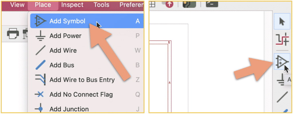
To drop a symbol to the editor sheet, you need to first bring up the symbol chooser window. The symbol chooser contains a listing of all available symbol libraries and their contents, as well as a search engine. You can look for a symbol by searching for it (if you know its name), or browsing for it. To bring up the symbol chooser, use the “A” hotkey, or choose the “Add Symbol” option under the “Place” top menu, or click the symbol button in the right toolbar (Figure 3.6.1).
The symbol chooser window will appear (Figure 3.6.2).

You can look for a symbol by typing a few letters of its name in the search box (1) or navigate the library and symbol list (2). In the example above, I am looking for the LED symbol, so I have typed “led” in the search box. The symbol chooser narrows down the contents of the listing pane (2) to symbols that contain “LED” in their name. I have clicked on the item in the first row. This prompts the symbol to appear in the symbol preview pane (3). Information about the selected symbol appears in the bottom left corner pane of the window. Some symbols also have associations with one or more footprints. You can choose one of the footprints by using the drop-down menu (4) and verifying that you have the correct association in the footprint preview pane (5). In my example, I don’t want to set an association at this time, so I leave the footprint dropdown unchanged and click OK (you may also double click on the device row (2) to select the symbol and dismiss the window).
After you dismiss the symbol chooser window, the symbol will be tied to the mouse cursor. You will be able to move the symbol around the editor. Find a good location for it, and then left-click to place it (Figure 3.6.3).

While a symbol is selected (you will see a bluish halo around it), you can use the “R” (counter-clockwise rotation) hotkey to change its orientation. You can select an unselected symbol by left-clicking on it. Remember that to un-select a selected symbol, simply left-click on any blank area. Also, to move a selected symbol, with the cursor over the selected symbol, press and hold the left mouse button and drag the symbol.
You can double-click on the symbol to bring up its properties window (Figure 3.6.4):
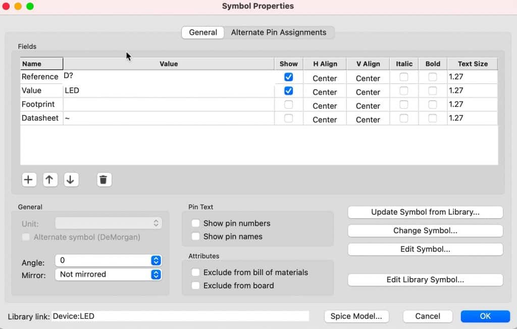
We will be editing the properties of this symbol later to do things such as assign a footprint or add a URL to a data sheet. For now, take a moment to become familiar with it, and click “OK” to dismiss it.
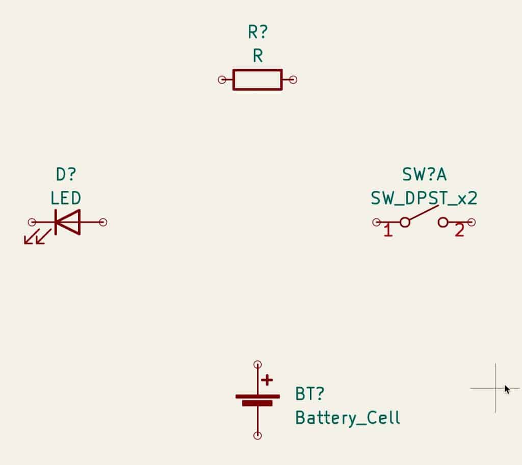
Repeat the process I described above to add the remaining symbols:
- Resistor (search for “R”).
- Switch (search for “SW_DPST_x2”).
- Battery (search for “Battery_Cell”).
Remember that you are working with symbols and that each symbol can be associated with a variety of “real life” footprints. For example, the battery symbol can be associated with footprints that belong to a 3.3V coin battery cell or a AA alkaline battery holder. We’ll do the associations later.
Once you have completed the addition of the four symbols, your schematic diagram will look like this (Figure 3.6.5):
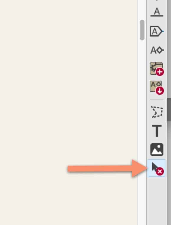
If you have made a mistake, it is easy to fix. Say that you changed your mind and want to replace a symbol with another. The easiest way is to delete the incorrect symbol by selecting it and hitting the “delete” key. Then use the symbol chooser to find the replacement symbol. You can also use the interactive delete tool from the right toolbar. Once you enable this tool, you can delete any item in the editor by clicking on it (Figure 3.6.6).
You can also change symbols in bulk. To learn more about this, please read the dedicated chapter on this topic.
The schematic editor now contains the four symbols I need for my simple circuit. I have not done the final placement and the wiring yet, as I’ll do that in the next two steps of the workflow.
For now, save the document, and continue with the next chapter.