Did you find an error in this page? Please report it. eBook version 12.
In Part 3 of the book (which you are reading now), you will learn about the basics of KiCad by working and completing a simple PCB project. In Part 3, the focus is on the schematic design, while in Part 4, the focus shifts to the layout design and the manufacturing. By the end of this project, you will have experienced the PCB design process using KiCad from start to finish.
While this first project is relatively simple, it will teach you the most important KiCad features and tools. You will develop skills that you will use in every future project regardless of its complexity.
As you work your way through this project, remember that you may need to reference the chapters in Part 13, Recipes, if you want to learn more details about specific features. To keep the size of the project concise, I have moved detailed descriptions of various features and tools to the end of the book.
The practical objective of this project is to design and manufacture a simple LED torch, like the one you see in 3.1.1 (below):

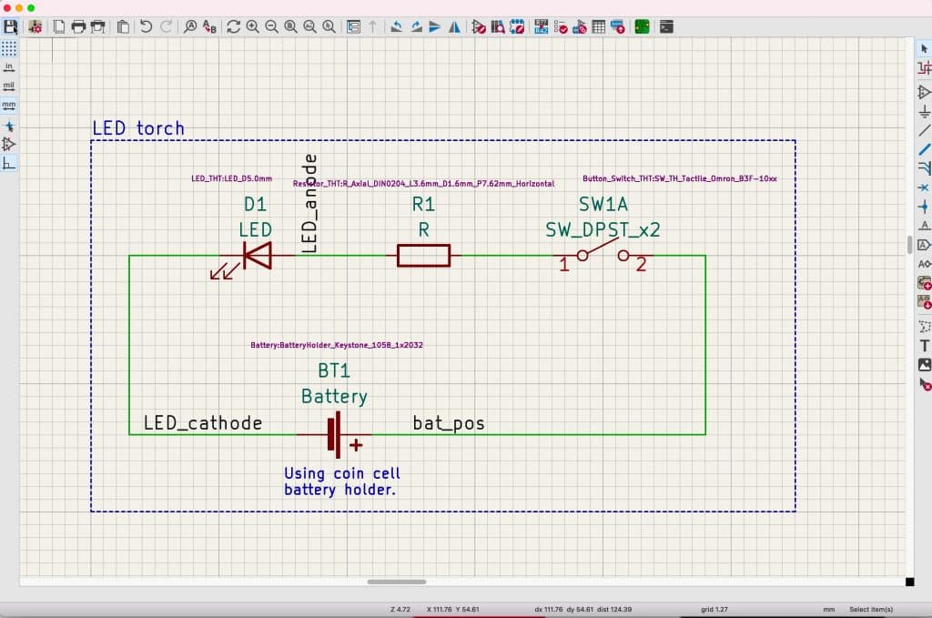
Most of the work will be in Eeschema (the schematic design editor) and Pcbnew (the layout design editor). At the end of this Part 3 of the book, the schematic design will look like this (Figure 3.1.2):
The final layout will look like this (Figure 3.1.3):

To guide the design of the PCB, I will be using the PCB design workflow that I outlined earlier in this book. I am also providing a summary in the next chapter.
The schematic (see Figure 3.1.2) contains only a few standard component symbols: an LED, a resistor, a button switch, and a battery holder. All these symbols are available in the KiCad libraries, so you will not need to get them from external sources. Electrically, the circuit contains a single loop. When you press the button, the circuit closes, and the LED turns on.
Despite this being a simple project, you will learn how to find and add symbols to the editor, associate them with layout footprints, annotate them, wire them, create named nets, run the Electrical Rules Checker, and decorate the schematic with text and graphics.
In Part 4, you will learn how to import the schematic in Pcbnew and design the physical layout, complete with beautifully rounded corners, mounting holes, silkscreen graphics, and, of course, pass the design rules check before sending it to manufacturing.