Did you find an error in this page? Please report it. eBook version 12.
In this chapter, you will complete step three of the schematic design workflow, that you learned about in the second chapter of this part of the book.
This chapter will show you how to arrange the symbols you added to the editor in their final positions, annotate them with unique reference IDs, and associate them with the appropriate footprints.
Arrange
Start by moving the symbols. After finding them in the symbol chooser, I simply placed the symbols in random locations in the previous chapter. Now, I will put them in locations that make it easy to wire them to become part of a valid circuit.
You can move a symbol by selecting it with your mouse, then click on the selected symbol and hold, while you move the mouse. The grid size and snap-to-grid function are important here. You can use the fast-switch grid size to experiment with the placement options. My fast-switch hotkey (Alt-1 and Alt-2) allow me to switch between 2.54 mm and 1.27 mm grid sizes. As the grid size becomes smaller, you can place the symbols with finer positioning control. For the circuit we are working on, 2.54 mm for the grid size is sufficient, so I’ll set it to that. You may also turn on the gridlines so that you can see the grid instead of only “feeling” it as a result of the snap-to-grid function.
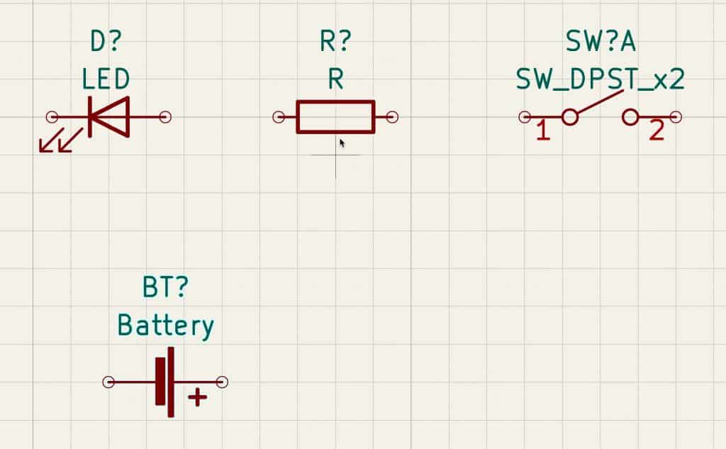
Go ahead and place the symbols as in Figure 3.7.1 (below).
Remember: you can rotate a symbol using the “R” hotkey after selecting it.
Annotate
Next, I will annotate the symbols. Annotation can be done manually or (preferable) automatic, and it entails setting unique reference IDs for each symbol.
First, what is the reference identifier? In Figure 3.7.1, notice that each symbol has a designator such as “D”, “R”, or “BT”, followed by a question mark. This is the symbol’s reference identifier. The reference identifier is a unique name for this symbol that we can use in the schematic and the bill of materials as an identifier for the symbol. The question mark indicates that the designator for the symbol is not yet set. To set it manually, double-click on the symbol to bring up its properties window (Figure 3.7.2).
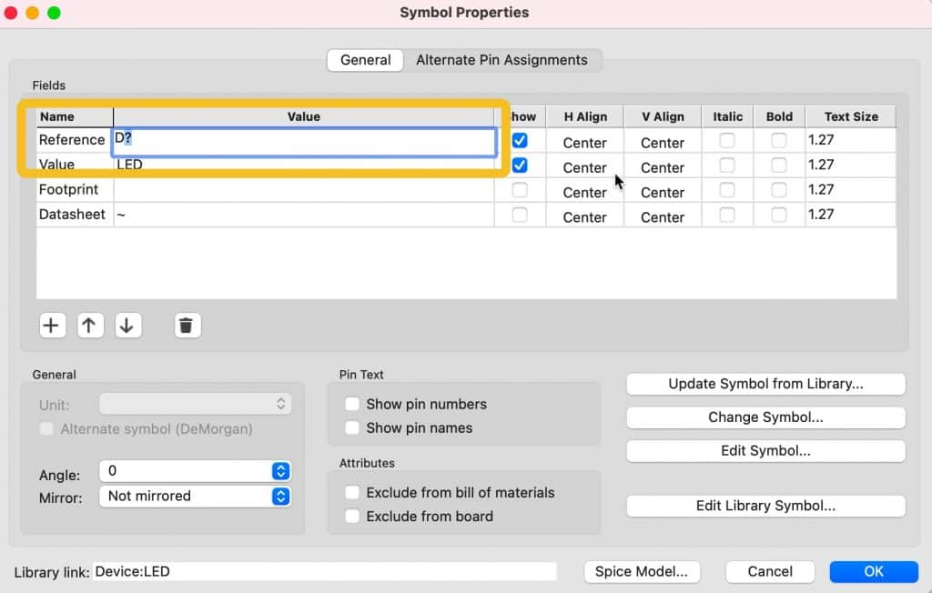
You can set the reference ID manually by editing the Reference field in the properties window. If you choose the manual method (which I discourage), you will have to keep track of the identifier assigned and ensure there are no duplicates. Click “Cancel” to dismiss the properties window.
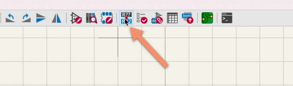
A better way to set the identifiers is to use the automatic annotator tool. Bring up the schematic annotator window by clicking the Annotator button from the top toolbar (Figure 3.7.3).
This will bring up the Annotator tool window that looks like this (Figure 3.7.4):

The default setting works well, and I rarely need to change them. Just click “Annotate” to let the tool set the reference IDs and then “Close” to dismiss the window.
Your schematic now looks like this (Figure 3.7.5):
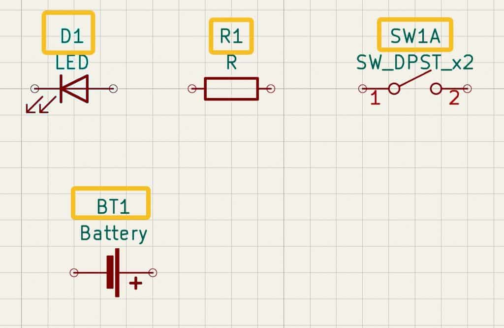
Notice that the question marks are replaced with numbers, and each symbol now has a unique identifier.
Associate
Next up, association. In association, we choose the desired footprint for a symbol. Remember that the footprint defines the physical attributes of a component in the schematic diagram. For example, take the resistor in Figure 3.7.5. What will this resistor look like in the final PCB? Will it be a through-hole component or an SMD? What will be its length and diameter? What are its silkscreen and other graphics?
There are several ways to associate a symbol with a footprint. You can assign a footprint, one symbol at a time, via the symbol’s properties window. For example, for the LED, double-click on the symbol to bring up its properties. In the properties window, notice the Footprint attribute (Figure 3.7.6).
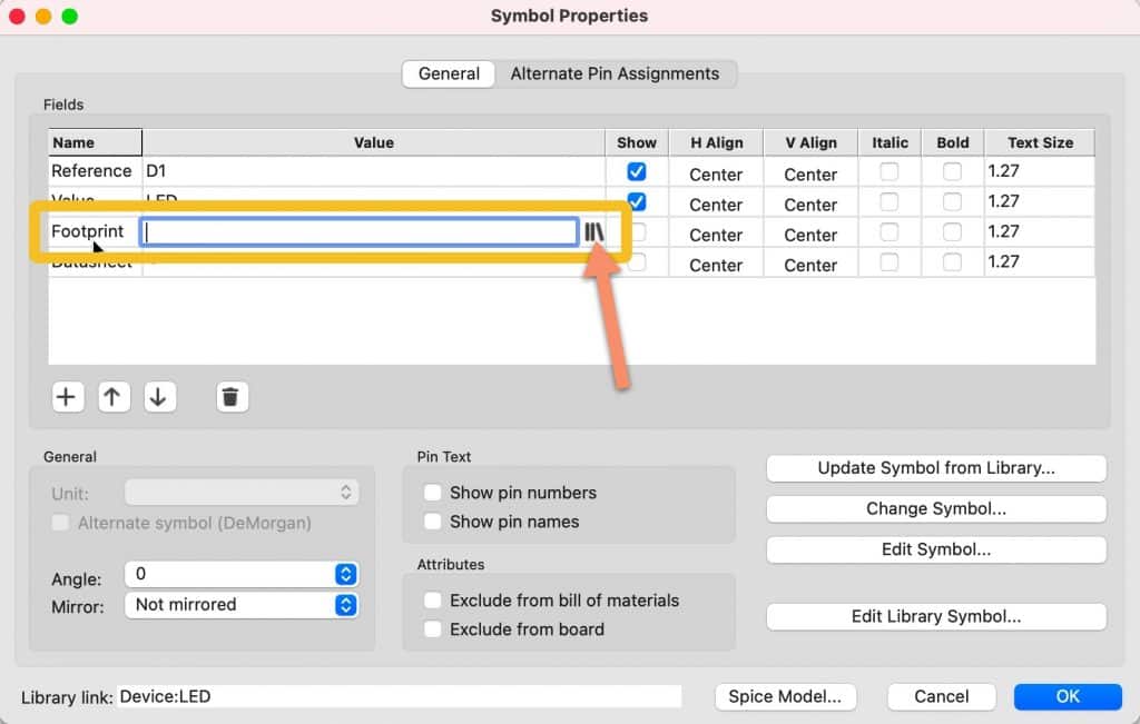
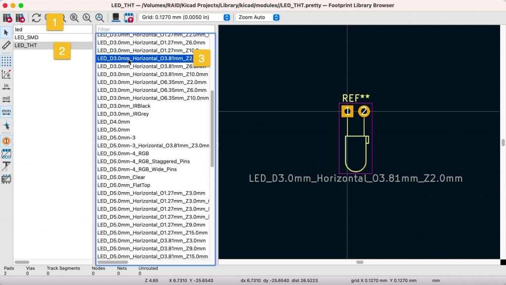
You can type the footprint identifier in the footprint field, although it is safer to click on the footprint library button to bring up the footprint chooser window (Figure 3.7.7). You can use the footprint chooser to search (1) and browse (2) for the desired footprint. Double-click to select it (3) and associate it with the symbol (4) when you find it. Before you close the symbol properties window, click on the “Show” check box of the Footprint property to display the footprint reference in the editor.
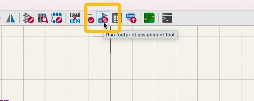
If your schematic only has a small number of symbols, this one-at-a-time method is sufficient. But for larger schematics, you will need a more streamlined approach. For this, Eeschema offers the association tool, which you can access from the top toolbar (Figure 3.7.8).
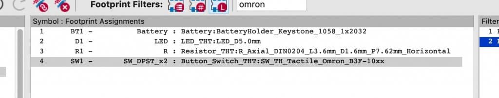
The associations tool contains three panes (Figure 3.7.9). The middle pane shows the symbols (left side) and their associated footprints (right). The left pane (1) contains a list of footprint libraries, and the right page (3) a list of footprints based on the selected library and the filter settings (top of the window). You can learn how to use the associations tool in detail by reading the dedicated chapter later in this book.

As you can see in the figure above, the LED symbol already has an associated footprint. I manually assigned this footprint earlier in this chapter. You can change this association by selecting the LED’s row and then double-clicking on an alternate footprint from the right pane (3). Also, notice that as you click on a symbol row in the middle pane, Eeschema pans the editor so that you can see the symbol in the schematic.
Let’s re-associate the LED symbol to an appropriate footprint. I have enabled all three filters (description, pins, and library) from the top menu bar. I have typed “led” in the search box. In the left library pane (1), I have selected the “LED_THT” library. In the right pane (3), you will see a listing of all footprints in the selected library and match my filter settings (Figure 3.7.10).

Double-click on the footprint in the right pane and notice how the association appears in the symbol row in the middle pane to finish the association.
Repeat the process so that all four symbols have their associated footprints. You can see my selected associations in Figure 3.7.11 (below).
My schematic editor now looks like this (Figure 3.7.12):

I have set the symbols to show their footprint properties (see earlier in this chapter on how to do this). I have also changed the appearance of the footprint property text to make it smaller. Learn how to do this in the relevant recipe chapter. With the symbol and footprint associations complete, step three of the process is also done. Let’s continue with the wiring in the next chapter.