Did you find an error in this page? Please report it. eBook version 12.
This chapter will give an overview of the model design workflow that I use to guide me through the PCB design process.
You can see the model in Figure 3.2.1 below. For a comprehensive discussion, please refer to Part 6 of this book, specifically Chapter One (the KiCad Schematic Design Workflow) and Chapter Two (the KiCad Layout Design Workflow).
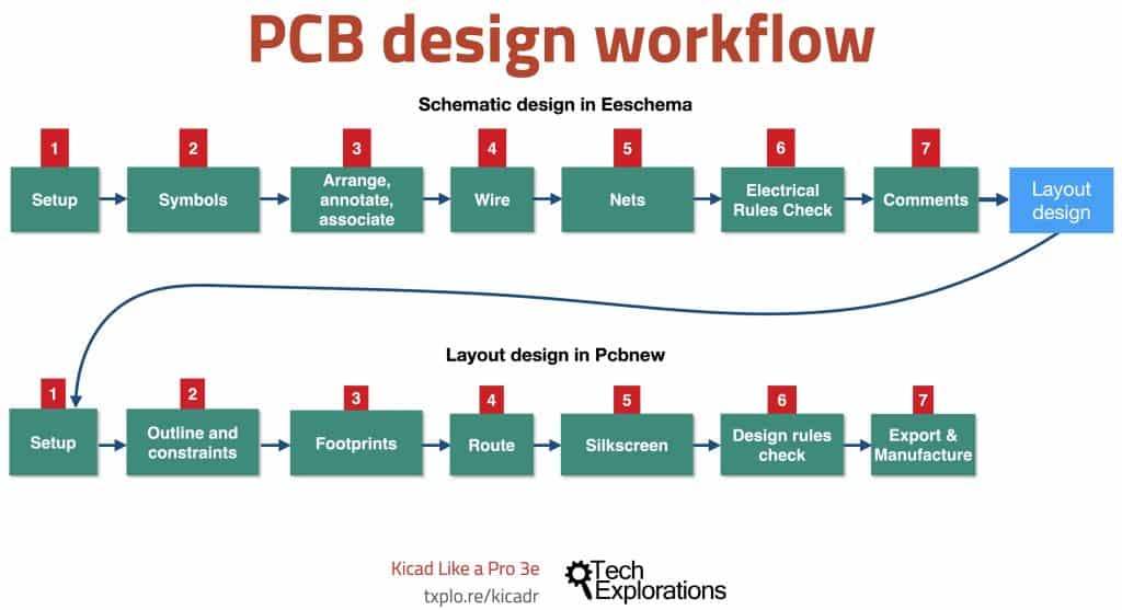
The model consists of two workflows: The Schematic Design Workflow and the Layout Design Workflow. We use Eeschema to create the schematic design and Pcbnew to create the layout design.
Throughout this first project, I will be referencing the steps you see in 3.2.1; you may want to bookmark this page to jump back here when you need to quickly.
As you can see, work begins in Eeschema. The schematic design workflow consists of 7 distinct steps, which you can complete linearly, one after the other. In real life, it is more common than not to iterate through these steps as needed. For example, you may need to change the wirings in step 4 after finding electrical errors in step 6.
When you complete the schematic design, you will continue with the layout design workflow using Pcbnew. Again, the layout design workflow consists of another seven distinct steps, which you can complete linearly. As with the schematic design workflow, real-life progression is typically iterative. It is common for a designer working in the layout design to jump to a much earlier step in the schematic design editor to fix a design bug, add new components, rewire, at make a change that affects the layout.
In this first book project, I will keep the workflows as linear as possible to reduce the overall complexity and improve your learning outcomes.
In Figure 3.2.2 (below), you can see a detailed depiction of the schematic design workflow. This depiction provides details about some of the tasks that we complete in each step.
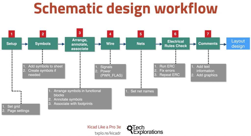
For example, you can see that in step four, you will draw the signal and power wires, while in step 5, you will set the names of the various nets. I will be helping you through each of the tasks in these seven steps through the project.
Similarly, in Figure 3.2.3 (below) you can see a detailed depiction of the layout workflow:
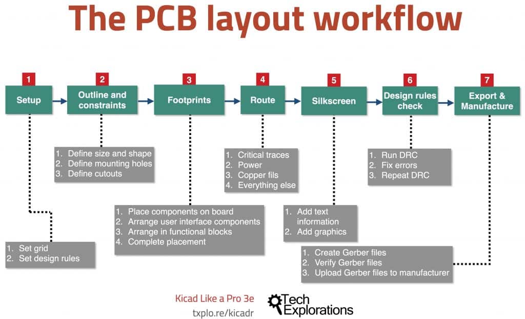
We will use the workflow in Figure 3.2.3 in Part 4 of this book which covers the layout workflow for this first project.